| Issue |
EPJ Nuclear Sci. Technol.
Volume 11, 2025
|
|
|---|---|---|
| Article Number | 23 | |
| Number of page(s) | 16 | |
| DOI | https://doi.org/10.1051/epjn/2025024 | |
| Published online | 04 June 2025 | |
https://doi.org/10.1051/epjn/2025024
Regular Article
In-core thermal and fast neutron measurements with 4H-SiC P+N junction diodes in the JSI TRIGA Mark II research reactor
1
Aix Marseille Univ, Université de Toulon, CNRS, IM2NP Marseille France
2
CEA/DES/IRESNE/DER, Section of Experimental Physics, Safety Tests and Instrumentation Cadarache F-13108 Saint Paul-lez-Durance France
3
Reactor Physics Division, Jožef Stefan Institute Ljubljana Slovenia
* e-mail: This email address is being protected from spambots. You need JavaScript enabled to view it.
Received:
12
July
2024
Received in final form:
5
February
2025
Accepted:
23
April
2025
Published online: 4 June 2025
Abstract
Accurate online in-core parameter measurements, such as neutron and photon fluxes and nuclear heating rates, are essential for fusion and fission applications. Wide bandgap semiconductors, particularly Silicon Carbide (SiC), have demonstrated strong potential for radiation detection over six decades. Despite this, challenges persist in optimizing detector performance under extreme in-core conditions. Our study focuses on 4H-SiC-based detectors, developed within a joint laboratory between Aix-Marseille University and the CEA, aiming to address these challenges and provide high-precision measurements for advanced nuclear facilities. Following previous measurements in ZPRs and with D-T neutron generators, this paper focuses on in-core experimental results obtained with such detectors in the Triangular Irradiation Channel (TIC) of the TRIGA Mark II-type research reactor at the Jožef Stefan Institute (JSI) in Slovenia. These in-core measurements were done by using two types of diodes. One with a Neutron Converter Layer (NCL) of Boron-10 for thermal neutron detection, and the other one without NCL in order to discriminate thermal and fast neutrons by studying 10B reaction versus scattering. Thanks to various Pulse Shape Analyses (PSA) and count rate studies the influence of bias voltage, NCL and neutron fluence on the detector performances were determined. The highest neutron flux and fluence for these detectors were reached: 1.2 × 1013 cm−2·s−1 and 1.2 × 1017 cm−2, respectively.
© V. Valero et al., Published by EDP Sciences, 2025
 This is an Open Access article distributed under the terms of the Creative Commons Attribution License (https://creativecommons.org/licenses/by/4.0), which permits unrestricted use, distribution, and reproduction in any medium, provided the original work is properly cited.
1. Introduction
In the 1970's, research in nuclear instrumentation focused on both gas detectors (such as ionization chambers and fission chambers) and solid-state detectors. These latter were composed of various standard semiconductor detectors such as Silicon (Si) or Germanium (Ge). However, another family of semiconductor has attracted a great deal of interest thanks to their physical and electronic properties: wide bandgap semiconductor. Among these latter are Silicon Carbide (SiC), III-V Nitrides, Diamond or Gallium Arsenide (GaAs). An important property that permits the use of wide bandgap semiconductors as radiation detectors is their lower intrinsic-carrier concentrations than that of Si semiconductor that induce very low leakage current. These semiconductors are widespread for applications with high-power, high-frequency, high-temperature and their use in harsh environments such as those that can be encountered in nuclear research reactors. Intense nuclear operating conditions for several purposes (safety, beam monitoring, nuclear physics or study of ageing of materials) are present in such facilities. Consequently, they can be used at higher temperature than those in Si, up to several hundred degrees. Regarding the place of SiC among the other wide bandgap semiconductors, it has many advantages for measurements in extreme environments. They are the The following are: high breakdown-electric field strength, rather high electron mobility, high thermal conductivity, high electron saturation velocity and a high stability versus radiation. Moreover, since the 90's, significant improvements were achieved about material quality through the development of SiC single crystals with a high-purity and epitaxial layers which have enabled the production of larger wafers [1–7].
Various poly-types of SiC exist. The most relevant for nuclear physics is the 4H one, among 3C and 6H [4]. Nowadays, 4H-SiC is the most used to design and develop thermal and/or fast neutron detectors due to its higher bandgap energy value as well as the resulting properties, and its availability on the market. Two main kinds of electronic devices are studied, the Schottky Barrier Diodes (SBD) and the P+N junction diodes. For thermal neutron detection, a Neutron Converter Layer (NCL), composed of specific materials with high thermal neutron absorption cross-sections, are needed. The most commonly used materials are Boron-10, Lithium-6 and Uranium-235. Other materials such as Nitrogen-14 can be also used for this purpose [1–5]. Such diodes (SBD and the P+N junction diodes) were exposed to various environments such as D-D and D-T neutron generators, neutron sources and neutrons fields from research reactors during ex-core and in-core experiments [2, 5–11]. SiC-based diodes were mostly tested under ex-core conditions and much less for in-core measurements for instance in TRIGA reactors [2, 5, 10]. Within the LIMMEX joint laboratory (Laboratory for Instrumentation and Measurements in Extreme Environment) between the CEA and Aix-Marseille University, 4H-SiC-based diodes are studied for a dozen years and promising results were obtained during D-T generators and Zero Power Reactor (ZPR) neutron measurements [12–16]. For instance, thermal neutron measurements thanks to these 4H-SiC-based detectors, have been carried out successfully in MINERVE (ZPR, CEA Cadarache, France) with a total neutron flux (thermal and fast) of 9.4 × 108 cm−2·s−1 [13], and thermal neutron fluence measurements has been conducted up to 2 × 1013 cm−2 into the spherical cavity of BR1 (ZPR, SCK-CEN, Belgium) [14].
Consequently, the new step was to characterize these 4H-SiC-based diodes under in-core conditions in a TRIGA reactor. The TRIGA Mark II-type research reactor of the JSI in Slovenia was selected for its ability to provide higher neutron fluxes and fluence values compared to previous experiments conducted with these detectors. These conditions are essential for evaluating the detectors’ performance under high-fluence scenarios. This paper presents the experimental results obtained in the Triangular Irradiation Channel (TIC) of this reactor.
The main objective of the irradiation campaign was to determine and compare the characteristics and performances of two types of 4H-SiC-based diodes: one fitted with a Boron-10 NCL for measuring thermal neutrons, and the other without an NCL for measuring epithermal and fast neutrons [17]. The study investigated the effect of bias voltage and neutron fluence on the response of the two detector types. A wide range of reactor power was considered, ranging from 0.2 W for functioning tests to full reactor power (i.e. 250 kW), corresponding to fluxes from 9.6 × 10⁸ to 1.2×1013 cm−2· s−1.
In this paper, the study SiC-based neutron detectors are detailed in their custom-made housing, designed especially for this purpose. Then, the irradiation conditions, the measurement set-up composed of the measurement chain and the studied SiC-based diodes, are explained. After these parts, the results are divided into two main sections. On one hand, the bias voltage influence on the count rate is shown as well as the effect of the NCL on the thermal neutron detection. On the other hand, the neutron fluence effects are shown thanks to a count rate study and a Pulse Shape Analysis (PSA). The amplitude, the charge, and some temporal characteristics: rise and decay time at 90% were evaluated. Finally, the radiation resistance of the detector is compared with data from the literature.
2. Studied SiC-based neutron detectors
Two types of SiC-based neutron detectors are studied, which have common features. First, they consist of the same P+N epi-junctions, growth on a 350 μm thick N+-type 4H-SiC substrate from a wafer provided from Ascatron (cf. Fig. 1). The N−-type epilayer is 20 μm-thick and has a low doping of approximately 2 × 1014 cm−3 with Nitrogen. This doping corresponds to the concentration of donor atoms. P+-type epilayer is 1 μm-thick and has a high Aluminum doping of around 1019 cm−3. The concentration of acceptor ions is 14 × 1021 cm−3, with an ionization coefficient of around 1%, since Al has a deep energy level in SiC typically located around 0.2 eV above the valence band [18, 19]. A stack of Ni/Ti/Al/Ni layers, 100 nm-thick, is then deposited and annealed to make the ohmic contact, which represents the anode. In order to reduce contact resistance, a 1 μm-thick layer of Al is then deposited using the electron beam evaporation technique. In the case of the first type of the studied SiC-based neutron detectors Boron-10 was directly implanted at 50 keV within the ohmic contact to create the NCL and to be able to detect thermal neutrons. Thus, the 10B concentration is around 2.2 × 1020 cm−3 but these atoms are stuck in the first 0.23 μm of the Al contact according to previous SRIM software (Stopping and Range of Ions in Matter) simulations [20, 21]. Finally, a metallic layer of Gold (Au), 555 nm-thick, was deposited on the surface of the detector. To make the cathode, a stack of Ti/Ni layers, 100 nm-thick, was deposited on the other side of the 4H-SiC substrate. In the case of the second type of detectors, no NCL is processed.
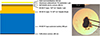 |
Fig. 1. Schematic (cross-section on the left-hand section) and picture (top view on the right-hand section) of the two types of the studied 4H-SiC-based diodes. |
These two types of diodes have circular patterns and similar surfaces. Dimensional measurements of the diodes were performed using a digital microscope with an imaging system, allowing for precise observation and measurement of their size and surface characteristics, and with a micrometric resolution. Three digits are inserted in order to show the small differences between diodes surfaces. For the diode with 10B NCL (called A), its diameter is 1.538 mm and its surface 1.858 mm2. For the diodes without NCL, called B and C, their diameters are 1.538 and 1.510 mm, and their surfaces 1.858 and 1.791 mm2, respectively. Two similar diodes without NCL have been used successively due to a loss of wire bonding for the diode B during the irradiation campaign. Consequently, the diode B in the housing was replaced by the diode C, which was mostly irradiated during this campaign. The two types of diodes are fixed onto an Alumina substrate and connected via Al bonding wires to pads in order to extract the electrical signal. With this design of the two studied 4H-SiC-based diodes, the Space Charge Region (SCR) corresponding to the sensitive part of the detector is located between the 1 μm P+-type epitaxial layer and the N-type epitaxial layer. It corresponds to the whole N-type layer when it reaches to maximum width, i.e. 20 μm for an applied reverse bias voltage of −68 V following calculations.
Concerning the physics principle of neutron measurement by these SiC-based detectors, in the case of a presence of a Boron-10 NCL, thermal neutrons are detected thanks to the high absorption cross-section of 10B: 3840 barns for 0.025 eV-neutrons. This reaction leads to the release of secondary charged particles, i.e. α particle (4He nuclei) and 7Li recoil nuclei. These particles lose all their energy within the successive very thin layers which compose the detector (from 100 nm for ohmic contacts to 350 μm for the substrate). Electron/hole pairs are created in the sensitive volume and are collected by the electrodes (also called ohmic contacts) positioned on both sides of the detector. This is made possible by means of an external applied electric field (bias voltage). For epithermal and fast neutrons, elastic, inelastic scattering or (n,α)/(n,p) reactions occurred. This is why the pulses are created due to interactions with mostly Silicon-28 and Carbon-12 nuclei.
In order to be able to carry out in-core measurements in the JSI TIC, it is essential to protect the diode from the strong electromagnetic disturbances induced by the external electromagnetic fields, and to be safeguarded against electrostatic discharges. Each diode is therefore housed in an encapsulation consisting of a base and a cover closed with screws. The design of the encapsulation was determined using 3-D numerical simulations of thermal and radiation-matter interactions. These works are detailed in [22, 23]. The base and cover of the housing are machined from a rod of Aluminum 6061 alloy. The thickness of the walls are identical at 1.5 mm and the housing is filled with Air. This alloy was chosen because it is composed of a low level of impurities (i.e. between 96 and 98.5% of pure Al), and because Aluminum-27 when irradiated has short half-life isotopes (i.e. 2.24 minutes for Aluminum-28 and 6.56 minutes for Aluminium-29). Grade 2 Titanium screws were chosen to close the housing and hold the diode in place. This material contains few impurities (over 99.3% Titanium) and the activated Titanium isotopes have short half-lives (i.e. 5.76 minutes for Titanium-51 and 1.71 minutes for Titanium-52). Then, a 6061 Al support was machined to fix the diode to the encapsulation and to raise the diode slightly to prevent its pads from touching the electrically conductive encapsulation and losing the signal. Two Alumina washers are positioned on either side of the diode to prevent the diode from moving with its vertically positioning (cf. Fig. 2). This encapsulation is not watertight, as the experiments carried out were done in the dry TIC (with ambient dry Air inside).
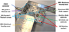 |
Fig. 2. Picture of an opened housing containing one type of 4H-SiC-based diodes. |
Then, the signal is transmitted via two conducting wires connected to the two diode pads corresponding to the anode and cathode and emerge from a custom-made connector from Thermocoax. This 316L Stainless Steel connector is screwed to the encapsulation via a threaded hole and locked to the connector via a nut. A mineral insulated coaxial cable is then used to transmit the signal from the connector to the acquisition chain, due to the harsh conditions encountered in the reactor core. Finally, a class 1, radiation-hardened, K-type Thermocouple with a diameter of 1 mm was integrated into the two separate housings to be positioned in the reactor core by means of a hole.
3. Experimental conditions and set-up
In this section, the experimental conditions of this in-core irradiation campaign are presented with some generalities about the JSI TRIGA Mark-II type research reactor. Then the whole measurement set-up from the detector to the final acquired is detailed.
3.1. Irradiation set-up
This section is dedicated to the general presentation of the TRIGA Mark II-type research reactor of the JSI [24–26], with its TIC and the associated experimental conditions.
The TRIGA (stands for Training, Research, Isotopes, General Atomics) Mark II reactor is a research reactor designed and built by the American company General Atomics. This reactor is well known for various fields of research such as detector development and testing, materials science, radiation damage, environmental sciences, nuclear data and nuclear computational codes [2, 10, 27]. TRIGA reactor designs make them ideal for educational purposes. Additionally, they are used for producing radioisotopes for medical and industrial applications. The JSI one is a pool-type reactor, which is not pressurized and for which cooling takes place by natural convection of light water inside the open pool. Its neutron reflector consists of a Graphite ring. Its nominal thermal power is equal to 250 kW. Several experiments with the two types of SiC-based detectors were realized for a wide range of powers (from 0.2 W to 250 kW) under steady mode with stable power.
Regarding the core (see Fig. 3), it is divided into 6 concentric rings A, B, C, D, E and F, with 1, 6, 12, 18, 24 and 30 locations respectively. Each location has a diameter of approximately 3.5 cm. About the core configuration which was present during the irradiation campaign, two Triangular Irradiation Channels were present and each takes the space of 3 locations (2 in the E ring and 1 in the D ring).
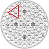 |
Fig. 3. Overall top view of the core with its different locations of the fuel elements, irradiation channels and control rods of the JSI TRIGA Mark II reactor, and with the Triangular Irradiation Channel used for the irradiation campaign (in red). |
The Triangular Irradiation Channel chosen for the detector study corresponds to the “old” one in the E10, E11 and D8 locations. This channel is named as such because it was the first to be installed at this location. It is characterized by its tubular shape with a quasi-triangular cross-section and its length of approximately 5.5 m. It rises from the core to the surface of the pool and is closed at the bottom to avoid the presence of water, as it is a dry channel filled with dry-air under natural convection. The channel is also curved by means of a bend which reduces the quantity and energy of radiation from the reactor core. This bend represents a challenge for the design of the detector-holders in order to integrate the devices and handle and move them as many times as necessary. As far as the internal dimensions of the channel are concerned, the main diagonals of the channel are approximately 7.7 cm and the internal diameter (without the triangular edges) is approximately 5.3 cm. Thanks to these mechanical characteristics a specific detector-holder was especially designed in order to center and fix the two types of diodes at the same axial position: the mid axial height of the core fuel elements. This detector-holder was manufactured either by 3-D-printing and made of Glycolyzed Polyethylene Terephthalate (PETG) or by the mechanical workshop with the custom-made Al 6061 one (see Fig. 4b). These detector-holders were especially designed for the TIC due to the special shape of the channel but also due to reactor operational constraints (PETG: up to 10 kW maximum and Al 6061: from 10 to 250 kW). The maximum operational constraints for PETG in a reactor core are primarily due to radiation damage, which degrades its molecular structure, as well as thermal constraints, as the material may lose its mechanical integrity due to its relatively low glass transition temperature of 80–85 °C. Calculations via the MCNP code were performed to determine the expected total neutron flux in the TIC [26]. The total neutron flux is 1.18 × 10¹³ (1 ± 0.0001) cm−2·s−1. Regarding the neutron flux distribution, according to Snoj et al., [25], 37.9% of neutrons are thermal (En < 0.625 eV), 29.4% are epithermal (0.625 eV < En < 0.1 MeV) and 32.7% are fast (En > 0.1 MeV). The reactor power is monitored using the reactor's built-in instrumentation. First, a fission neutron counter is used to monitor the reactor start-up (from 0.05 mW to 50 W). A compensated ionization chamber then tracks the power evolution linearly (from 100 mW to 300 kW), followed by another compensated ionization chamber operating on a logarithmic scale (from 1 W to 1 MW) [24].
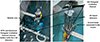 |
Fig. 4. Pictures showing the positioning of the two SiC-based detectors in the TIC thanks to the detector holders. |
3.2. Measurement set-up
The measurement set-up is composed firstly of the two types of 4H-SiC-based neutron detectors, one with 10B NCL and the other without, described in the previous section. As shown in Figure 4, these two individually-encapsulated detectors are inserted in the specific 3-D detector-holder in order to integrate the diodes in the TIC channel. Three SiC-based diodes were studied, one with NCL (diode A) and two bare ones: diode C was used as a replacement for diode B. Moreover, two detector-holders made of different materials (PETG/Al 6061) but with similar dimensions were used for the measurements.
Then, two 10 m-length mineral insulated coaxial cables (one per detector), with a 50 Ω impedance, are used in order to distribute the signal from the detector in the reactor pool to the platform. In order to be able to carry out measurements in this TRIGA reactor and at high neutron flux values expected (up to 1.2 × 1013 cm−2·s−1), a dedicated fast conditioning and acquisition chain has been set up (see Fig. 5) to be able to operate in pulse mode. The current operating mode was not used during these experiments due to the maximum neutron and photon flux values tested which are not important enough to use it.
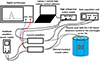 |
Fig. 5. Schematic of the measurement chain used in the Triangular Irradiation Channel. |
Two current amplifiers (CIVIDEC Instrumentation, C2 HV and TCT) are used in order to amplify (40 dB gain) the pulses generated by γ and neutrons which are coming from the detector. These front-end current amplifiers are powered by a stabilized power supply (TTi, EL303R) and connected to a high voltage power supply for detector biasing (CAEN, DT5533EM). The latter is monitored by a laptop with a dedicated remote operation software (CAEN, GECO 2020). Finally, the amplified signal coming from each current amplifier is displayed and recorded by means of a 20 GHz-sampling rate digital oscilloscope (Agilent, MSO9104A). When the pulse amplitude is higher than the trigger threshold, fixed at +19 mV, the pulse is recorded and stored into binary files. The advantage of pulse recording is the possibility to achieve a PSA. This kind of amplifier integrates the current pulse and outputs a voltage pulse whose amplitude is proportional to the charge of the input pulse. The study of the detector characteristics is made possible in greater depth than with the use of a more standard measurement chain with a Multi-Channel Analyzer (MCA) and/or with a charge amplifier.
For the different count rates acquired, the hypothesis of a Poisson distribution-like behavior of raw count rate has been done. Thus, the uncertainty corresponds to the inverse of the square root of the number of pulses recorded, which is then multiplied to the count rate. Finally, this is multiplied by 2 in order to obtain the expanded uncertainty (k=2 and confidence level = 0.95).
Due to the addition of K-type Thermocouples, a data acquisition unit (Agilent, 34970A) with a multiplexor (Agilent, 34901A) was also used in order to measure the temperature inside each SiC-based detector.
4. Results
In this section, the results obtained during this irradiation campaign are detailed with a first part dedicated to bias voltage and NCL influences on the count rates and a second part focusing on the diode behaviors as a function of power and fluence effect on ethe count rates and on the pulse characteristics. These pulse characteristics are determined and analyzed thanks to a MATLAB script using Signal Processing Toolbox. Their main characteristics of interest are amplitude, rise time and decay times at 90%, and the deposited charge.
4.1. Detector behavior with bias voltage and influence of the NCL
The first aim in this irradiation campaign was to study the influence of the bias voltage and the NCL on the response of the two SiC-based diodes. The aim was to determine the optimum bias voltage in order to reach a Charge Collection Efficiency (CCE) very close to 100%. The presence of the Neutron Conversion Layer (NCL) may have a significant impact on charge collection, as it could influence the generation and transport of charge carriers within the diode. This effect is one of the hypotheses tested in this study, the aim of understanding is how the NCL affects the overall detector performance under irradiation. To do this, the saturation curve of the count rate for a reactor power of 100 W and corresponding to a total neutron flux, of approximately 4.8 × 109 cm−2·s−1 was studied for the two diodes for a bias voltage ranging from 0 V to −600 V. The results are plotted in Figure 6. The two diodes have the same behavior. Their count rates increase and reach a plateau from −300 V. This plateau is characteristic of a 100% CCE value.
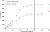 |
Fig. 6. Evolution of the count rates of the A (in blue) and B (in red) SiC-based diodes versus the reverse bias voltage for a reactor power of 100 W in the Triangular Irradiation Channel and with a mean temperature of around 23.1 °C. |
Moreover, a significant difference in the count rate is observed between diode A, which includes a Boron-10 NCL, and diode B, which does not. The count rate of diode A is consistently higher than that of diode B. As shown in Table 1, the difference remains stable when the charge collection efficiency (CCE) is at 100%, from −300 to −450 V. At 600 V, only diode B experiences a sharp increase in count rate which can be characteristic of another operation regime. However, the lack of data points at higher voltages prevents drawing definitive conclusions. The mean difference between the count rates is 2299 s−1, considering the results obtained between −300 and −450 V.
Count rates (s−1) of the A and B SiC-based diodes for five different reverse bias voltages for a reactor power of 100 W in the Triangular Irradiation Channel.
Since the diodes are positioned at the same axial height, have the same surface area, and similar active areas, this difference can be attributed to the presence of the NCL on diode A. Consequently, diode A, thanks to this conversion layer, is capable of detecting thermal neutrons in addition to epithermal and fast neutrons, whereas diode B only detects epithermal and fast neutron fluence. While this finding does not conclusively prove the hypothesis, it supports a straightforward explanation: the presence of the NCL significantly enhances the sensitivity of diode A to thermal neutrons.
These curves allowed the choice of the bias voltage applied for the next measurements of the irradiation campaign to be in the plateau. A −400 V bias voltage value was chosen.
Due to the loss of wire bonding of diode B, the diode C was also characterized with diode A for the same reverse bias voltages values. An identical behavior was obtained with a higher count rate for diode A versus diode C.
4.2. Behavior as a function of power and fluence
After determining the influence of the bias voltage on the diode responses, experiments were carried out at the selected bias of −400 V. The second aspect of our study focuses on the effects of neutron fluence on the detector characteristics and, consequently, their radiation resistance.
4.2.1. Count rate
Count rate study was followed during the whole irradiation campaign and for a same bias voltage, i.e. −400 V. Experiments were realized for reactor powers ranging from 100 W to 250 kW corresponding to a total neutron flux from around 4.8 × 10⁹ to 1.2 × 1013 cm−2·s−1. The objective of these measurements was to expose the diodes to a high neutron fluence to assess the presence of defects that could potentially reduce their detection efficiency, and which is more than mentioned in the literature. This approach aimed to evaluate the impact of radiation damage on the detection efficiency of our diodes, by studying the count rate evolution as a first approach. In principle, if the detector is unaffected, the count rate will remain stable and increase linearly with rector power. 100 k pulses were acquired in total due to lower count rates, as such statistics were deemed sufficient for the purpose at hand. In addition, several acquisitions were carried out for the same power in order to observe the count rate evolution. To ensure the count rates were comparable to those recorded at −400 V during the bias voltage study, the background count rate difference was subtracted from the measurements for both diodes.
The variation of the count rate normalized per reactor power and plotted versus the neutron fluence is detailed in Figure 7a and 7b for the diode A and C, respectively with and without NCL. This curve is composed of four phases, and the corresponding count rate values are presented in Table 2a. For the first phase at low neutron fluence values (up to 1 × 1014 cm−2), the normalized count rate corresponding to 100 and 200 W decrease with a same slope. For the second phase at intermediate neutron fluence values (from 1 × 10¹⁴ to 2.1 × 1015 cm−2), the count rate still decreases with a same slope for powers ranging from 1 kW to 20 kW for day 1. A drift is observed for each reactor power. The third phase is presents at higher neutron fluence values (from 3.2 × 10¹⁵ to 2 × 1016 cm−2), for reactor powers from 20 kW to 100 kW for day 2. Finally, the last slope is visible up to 1.2 × 1017 cm−2, and the normalized count rate continues to decrease until reaching values lower than 0.1 s−1·W−1.
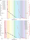 |
Fig. 7. Count rate of the diode A with NCL (a) and diode C without NCL (b) normalized by reactor power versus the neutron fluence for power ranging from 100 W to 250 kW in the Triangular Irradiation Channel for an applied bias voltage of −400 V, and for day 1 (in black) and day 2 (in red). |
Count rate degradation induced by neutron fluence for diodes A (a) and C (b).
The same behavior was also observed for the diode C without NCL and the count rates values and drifts are presented in Table 2b. A similar decrease for the normalized count rate and degradation for high neutron fluence values are observed for both diodes with and without NCL. For diode C, a lower count rate normalized by reactor is observed for 200 W than for 1 kW. This behavior can be interpreted by the damages caused by epithermal and fast neutrons, creating deep defects in the crystal lattice of SiC, which may lead to the compensation of dopant atoms of the epilayer [28]. This degradation induced a change of the pulse shape too. The latter is detailed in the following section.
Moreover, a higher count rate was obtained for the diode A with NCL due to thermal neutron detection as already observed in the previous section regarding bias voltage influence.
As observed in Table 2a and 2b, a strong decrease of count rate versus neutron fluence and especially from 3 × 1015 cm−2 is present for the experimental conditions and the operating protocol used. This behavior is materialized by the increase in the count rate drift and the presence of strong values of relative drift. Thus, for the first phase, the mean count rate increases with reactor power except for one point at 200 W for diode C. The relative drift is much higher for the diode C, without NCL. For the second phase, the mean count rate continues to increase with reactor power for both diodes. The count rate drift and relative drift reached their maximum values in this phase for 10 kW. The mean relative gap is less important in this phase than for the first one with a mean of −19.5% and −17.9% for diode A, and −44.6% and −20.6% for diode C, respectively. For the last phase, the mean count rate decreases from 50 kW for diode A and from 20 kW from diode C. The most visible drop in the count rate is observed between 5.3 × 1015 cm−2 and 2.5 × 1016 cm−2 for both diodes. This range is well known in the literature and will be described in the last section of this paper. The relative drift increases with neutron fluence, except for 100 kW. This behavior proved fluence effect on count rate.
The behavior of the count rate with increasing power is qualitatively equivalent for both diodes, despite the differences in their absolute count rates. This suggests that the underlying mechanisms influencing the count rate, such as charge trapping by defects strongly increased by neutron fluence, are consistent across both detectors. The observed deviations from expected stability are addressed in the literature [28, 29], and further investigations are planned to quantify these effects more rigorously, such as the achievement of Deep Level Transient Spectroscopy (DLTS) measurements on these studies SiC-based diodes. The DLTS analysis allows the measurement of the defect carrier concentration and their binding energy in the SCR of semiconductor materials, in order to investigate the nature of the defects (concentration, energies and type) induced by neutrons during these experiments.
4.2.2. Pulse Shape
After showing the evolution of the count rate for the whole reactor powers tested and its drop due a potential increased defect concentration in the SiC, the neutron fluence effects on the pulse shapes is presented.
Such as the decrease of count rate with fluence, the amplitude is also impacted by this parameter, as presented in Figure 8 with the recorded pulses for diodes A and C. The number of total pulses acquired was at least 60 k for each power. This qualitative analysis clearly highlighted that the neutron fluence has an influence on the general shape of the pulses. This is particularly the case for their maximum amplitude, also called height. Indeed, for a fluence value of around 7 × 1016 cm−2, the pulses have amplitudes varying between 0.04 and 0.06 V maximum. It is not the case for a 1 × 1015 cm−2 fluence, where some pulses have amplitudes much higher than 0.06 V (the biggest ones are cut due to the Oscilloscope window). The behavior is identical for the two SiC-based diodes, with and without NCL and confirms the effect of neutron fluence on some pulse characteristics of the detectors. In fact, deep defects are created and caused by elastic and inelastic scatterings (fast neutrons). They are suspected to be responsible of such behaviors. It has to be noticed that the general shape and width of the count rate response remain unaffected across the tested conditions, with only the amplitude varying. In fact, the pulse shapes for the two SiC-based diodes seem similar. At lower reactor powers, such as 10 kW, a large spread in amplitude is observed, whereas this spread becomes negligible at the maximum tested power of 250 kW. This indicates that the observed variations are primarily amplitude-dependent and not due to changes in the detector response. A few quasi-rectangular pulses, at a mean value of around 0.04 to 0.06 V, can be discriminated thanks to the detection of secondary charged particles from the NCL (thermal neutrons) such as explained in [30] in the case of a single crystalline CVD Diamond. This is not the case for the highest peaks visible at 10 kW which are cut-off because the diode signal is exiting the acquisition window of the oscilloscope. Moreover, the charge deposited, which corresponds to the area under the plot, also decreases as the amplitude decreases. This observation is confirmed by analyzing the charge histograms, which exhibit consistent behavior. These histograms, included in the Appendix (cf. Fig. A.1), further validate the conclusion that the observed changes are predominantly driven by variations in the amplitude. Thanks to the link between these two parameters of interest, the next section will focus on the analysis of the maximum amplitude (i.e. height) distribution of pulses as function of neutron fluence..
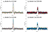 |
Fig. 8. Pulses of the diode A for reactor powers of 10 kW (a) and 250 kW (b) with neutron fluences of 1.1 × 1015 cm−2 and 6.6 × 1016 cm−2 respectively, pulses of the diode C for reactor powers of 10 kW (c) and 250 kW (d) with neutron fluences of 1.1 × 1015 cm−2 and 7.6 × 1016 cm−2 respectively (bias voltage of −400 V). |
4.2.3. Pulse Height Analysis (PHA)
A quantitative analysis of the pulse height was realized. The term Pulse Height Analysis is widely spread and encountered in the literature to refer to these type of analysis. Its distribution, also called Pulse Height Distribution (PHD), was plotted in Figure 10 for the two types of diodes, namely A and C. These fluences were selected for diodes A and C in order to deepen and extend the values encountered in the literature. Moreover, this range of fluences was selected to cover the measurement interval from the fluence at which the diodes begin to experience a significant drop in their count rate to the maximum fluence received by the detectors, in order to observe the changes highlighted in the two previous result subsections. They are the following: 3.2 × 10¹⁵, 1.1–1.2 × 10¹⁶, 2.8–2.9 × 10¹⁶ and 6.6–7.6 × 1016 cm−2. These values were obtained for reactor powers of 20, 100, 150 kW and 250 kW, i.e. full power. As noticed in Figure 9, the same behavior is also observed with the decrease of amplitude. Before discussing the results, it is important to introduce the concept of folding. Folding occurs when pulse amplitude decreases due to limitations caused by defects induced by neutrons in the diodes. This phenomenon is evident in the PHD and corresponds to a folding phenomenon. A same trend is shown for diodes A and C with and without NCL, respectively. This phenomenon corresponds to a decrease of the CCE, which cannot reach again its initial value (permanent damage due to defects) of 100% because the path of particles with charge collection is reduced. Such a plot permits to put forward the assumptions made in the previous sections regarding neutron fluence effects with the decrease on count rate and pulse height with the pulse shape observation. Moreover, the presence of a protrusion has to be reported for the diode A with NCL, and 20 kW (cf. red circle in Fig. 9) and 50 kW reactor powers (not shown). The latter, which can be characteristic of the NCL, moved when neutron fluence increases because of the folding phenomenon, but more investigations are needed in order to deepen this shift. In fact, as the neutron fluence increases, there is a shift toward lower amplitudes across all pulse amplitudes. In more general terms, this Pulse Height representation is mainly made up of elastic collisions, inelastic collisions on Silicon-28 and the component linked to γ rays (at the beginning of the spectrum), which can be discriminated. As a reminder, identical results were obtained for the charge histograms for both diodes and can highlight a relationship between amplitude and charge with neutron irradiation.
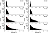 |
Fig. 9. Pulse Height Distribution of the A (on the left-hand section) and C (on the right-hand section) SiC-based diodes for power ranging from 20 to 250 kW and neutron fluences from around 3.2 × 10¹⁵ to 6.6–7.6 × 1016 cm−2 with 100 k pulses recorded, and for a bias voltage of −400 V. |
4.2.4. Rise and decay times analysis
The last part of the study of fluence effects focused on some temporal characteristics of the SiC-based diodes: rise and decay times at 90%. The rise and decay times at 90% were selected as the most reliable detector parameters characteristic of the signal dynamics, particularly in response to neutron fluence. They provide a clear representation of the signals rise and fall, making them ideal for assessing the detectors performance. Indeed, it was useful to know if such characteristics can be affected by fluence such as for the amplitude and the deposited charge. As a reminder, in Section 4.2.2, the shape was already observed to remain unchanged in width. However, in this case, the analysis goes beyond qualitative observations. In fact, if these times are remaining constant with fluence, the detector will be able to keep its fast response. It is also possible to prevent pile-up effect and to helps to focus only on the amplitude decrease as outlook. Therefore, since a single population was observed for the two key characteristics in both diodes, the mean values are plotted in Figure 1 for diodes A and C.
The same fluences and reactor powers as the PHD were studied. A similar behavior for the two diodes can be seen in Figure 10. In fact, the rise and decay times remained stable as a function of neutron fluence, putting forward that they are unaffected by such a parameter. It can be concluded that the latter are not influenced by the neutron irradiation up to 8 × 1016 cm−2. Finally, the only difference between the diodes was that A has slightly higher rise and decay times at 90% compared with C without NCL. This means that the pulses from diode C rise and fall faster than those from diode A. An explanation for this temporal difference with and without NCL could be: thermal neutron detection through the NCL slows down the full signal. However, further investigations are needed to explore this approach, which could potentially serve as an additional method for distinguishing between different detector behaviors. Such investigations may be performed via the use of a faster measurement chain with homemade electronics.
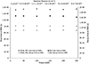 |
Fig. 10. Rise and decay times at 90% mean values for the two SiC-based diodes (A and C) as function of neutron fluence for a bias voltage of −400 V. |
4.2.5. Neutron irradiation induced defects
The impact of neutron fluence on detector performance has been analyzed based on previous studies. Ruddy et al. observed, for similar detectors and experimental conditions, a decrease in pulse amplitude due to defects induced by fast fission neutrons energy (En > 1 MeV), the count rate remaining constant up to a neutron fluence of 1.7×1017 cm−2 [28, 29]. In our case, a drop in count rate was observed. This can be explained by the fact that as the pulse amplitude decreases, a significant number of pulses fall below the oscilloscope trigger threshold and are then no longer detected.
According to Ruddy et al., the amplitude quickly decreases above 1014 cm−2 with pulses tending to approach the background noise amplitude at higher fluences [29, 31]. One possible solution to mitigate this issue would be to increase the amplifier gain, combined with background noise rejection through a dedicated PSA script.
When SiC is irradiated, defects are introduced into the crystal lattice, acting as carrier traps. Charge carriers are then recombined as their trapping times become comparable to or shorter than their transit times in SiC, preventing their collection and thereby reducing the CCE. This mechanism has been extensively studied in the literature, particularly through Deep-Level Transient Spectroscopy (DLTS) analyses [32]. Nava et al. [33] identified deep defects in SiC at ionization energies of Ec − 1.16 eV and Ec − 1.50 eV, with trapping times comparable to or shorter than carrier transit times. These defects are associated with C vacancies (VC) and complexes involving both C and Si vacancies (VC +VSi). Their formation depends on the energy of the incident particle, with threshold energies between 100 and 200 keV for C and between 200 and 300 keV for Si [34]. The most detrimental defect for detector performance, known as Z1/2, corresponds to C vacancy complexes.
Additionally, for neutron fluences exceeding 1015 cm−2, SiC becomes intrinsic or semi-insulating. This is consistent with our results, as a strong count rate reduction is observed between 1 and 3 × 1015 cm−2, which corresponds to a significant drop in the doping concentration of the sensitive N-type layer. Depending on the authors, the CCE decreases by 80% or 50% for fluences of 8 × 1015 cm−2 and 2 × 1016 cm−2, respectively [33, 35]. The presence of an increasingly heterogeneous electric field within the diode makes charge collection more difficult. Despite this CCE reduction, the detectors continue to operate, as the density of traps surpasses the initial carrier concentration, leading to a proportional decrease in the effective doping concentration (Neff) with neutron fluence [29]. One potential countermeasure is to increase the bias voltage to enhance carrier mobility and facilitate their collection [33]. Another approach would be thermal annealing at around 300 °C, which has been reported to mitigate the impact of Z1/2 defects on epilayer doping compensation [29, 35]. In our case, the maximum temperature reached was below 100 °C at full reactor power, which was insufficient for this effect to take place.
4.3. Conclusion and outlooks
This study presents the results obtained with two SiC-based detectors, one with and one without NCL, during an in-core irradiation campaign at the TRIGA Mark II research reactor of the JSI in Slovenia. This work represents the first in-core measurements conducted in a research reactor using these LIMMEX detectors. The neutron flux and fluence reached in this experiment were about 104 times higher than those of previous studies involving these detectors, marking a significant achievement for our devices. The SiC-based detectors, which have similar surface areas and are fitted with or without Boron-10 NCL, were successfully tested thanks to a newly developed fast acquisition chain operating in pulse mode.
A saturation study conducted in this neutron field confirmed thermal neutron detection, count rates being compared between the diode with NCL and the diode without NCL. The optimal bias voltage to achieve a CCE close to 100% was determined to be −400 V, where the count rate saturated. The impact of neutron fluence on sensor characteristics was then explored through three different phases in the count rate analysis. A significant decrease in the count rate as a function of neutron fluence was observed, with a dynamic depending on the phases (i.e. fluence range). A similar behavior was noted for both SiC-based diodes, regardless of the presence of NCL. These notable decreases occurred between 1 × 10¹⁵ and 3 × 1015 cm−2, which aligns with literature reports of defects created by neutron irradiation.
Regarding the pulse shapes, high-amplitude pulses were recorded for both diodes, characteristic of fast fission neutron interactions, which occur due to elastic and inelastic scatterings. Some quasi-rectangular pulses, typical of thermal neutron detection, were observed in the diode with NCL, highlighting the discrimination capability of these detectors. Thermal neutron detection and the impact of neutron fluence were further supported by the PHD plots, which showed a peak and a folding phenomenon. The temporal characteristics of the pulses remained unaffected by fluence, in contrast to the amplitude and charge, which decreased. This result is promising, as it suggests that the detectors will maintain their fast response and be able to prevent pile-up effects even at fluences up to 8 × 1016 cm−2.
Following the literature, the significant reduction in count rate, amplitude, and charge is attributed to the formation of deep-level defects such as the Z1/2 defect, induced by fast fission neutrons. This leads to a decrease in the effective doping concentration (Neff) and to an intrinsic material.
Regarding future prospects, a short-term goal would be to perform DLTS measurements on the SiC-based diodes studied here, to investigate the types of defects induced by neutrons. In the medium term, experiments with a current amplifier featuring adjustable gain could be conducted to increase pulse amplitudes. Additionally, it would be beneficial to study the effect of increasing the bias voltage when CCE decreases, as well as design a heating system to compensate the Neff decreasing effect. In the long term, coupling the SiC-based diodes with other detectors, such as a single-cell calorimeter or a fission chamber, within a multi-sensor probe could be a valuable direction. This would enable measurements of the neutron flux and absorbed dose rate (also known as nuclear heating rate), which could be compared with values obtained using radiation-matter interaction calculation codes.
Acknowledgments
The authors want to thank the JSI and Reactor Physics Department (F8) team for their welcome and their warm support during the whole irradiation campaign. Finally, the authors want to thank Mr. Frédéric Derivaux, from the Mechanical and Micro-Mechanical Workshop of the IM2NP laboratory, for its support and the realization of the various SiC-based diodes encapsulations without which these measurements could not have been ensured.
Funding
This work has been performed during a 3-months PhD international mobility founded by the ISFIN Institute. The project leading to this publication has received funding from the Excellence Initiative of Aix-Marseille University - A*Midex, a French “Investissements d’Avenir programme” AMX-19-IET-013.
Conflicts of interest
The authors declare that they have no competing interests to report.
Data availability statement
This article has no associated data generated and/or analyzed/Data associated with this article cannot be disclosed due to legal/ethical/other reason.
Author contribution statement
Valentin Valero: writing – original draft, formal analysis, data curation, visualization. Laurent Ottaviani: conceptualisation, investigation, validation, supervision. Abdallah Lyoussi: conceptualisation, investigation, validation. Christophe Destouches: validation, resources. Vladimir Radulović: methodology, supervision, resources. Luka Snoj: supervision, resources. Adrien Volte: resources, investigation, visualization, supervision. Michel Carette: software, visualization, data curation. Christelle Reynard-Carette: writing – review and editing, software, founding acquisition, methodology, validation, supervision.
References
- R.R. Ferber, G.N. Hamilton, Silicon carbide high-temperature neutron detectors for reactor instrumentation, Nucl. Appl. 2, 3 (1966) [Google Scholar]
- J. Coutinho, V.J.B. Torres, I. Capan, T. Brodar, Z. Ereš, R. Bernat, V. Radulović, K. Ambrožič, L. Snoj, Ž. Pastuović, A. Sarbutt, T. Ohshima, Y. Yamazaki, T. Makino, Silicon carbide diodes for neutron detection, Nucl. Instrum. Methods Phys. Res., Sect. A 986, 164793 (2021) [CrossRef] [Google Scholar]
- I. Capan, Wide-Bandgap semiconductors for radiation detection: A review, Materials 17, 1147 (2024) [CrossRef] [Google Scholar]
- M. De Napoli, SiC detectors: A review on the use of silicon carbide as radiation detection material, Front. Phys. 10, 898833 (2022) [CrossRef] [Google Scholar]
- R. Bedogni, A. Calamida, A.I. Castro Campoy, A. Fontanilla, J.M. Gomez-Ros, V. Monti, E. Mafucci, N. Protti, S. Altieri, A. Pietropaolo, On neutron detection with silicon carbide and its resistance to large accumulated fluence, Eur. Phys. J. Plus 137, 1358 (2022) [CrossRef] [Google Scholar]
- C. Raynaud, Propriétés physiques et électroniques du carbure de silicium (SiC), Techniques de l’Ingénieur (Éditions Techniques de l’ingénieur, Energie, D3119 V1, 1, 2007) [Google Scholar]
- A. Owens, Semiconductor Radiation Detectors, 1st edn. (CRC press, 2019) [CrossRef] [Google Scholar]
- M. Rebai, D. Rigamonti, S. Cancelli, G. Croci, G. Gorini, E. Perelli Cippo, O. Putignano, M. Tardocchi, C. Altana, M. Angelone, G. Borghi, M. Boscardin, C. Ciampi, G.A.P. Cirrone, A. Fazzi, D. Giove, L. Labate, G. Lanzalone, F. La Via, S. Loreti, A. Muoio, P. Ottanelli, G. Pasquali, M. Pillon, S.M.R. Puglia, A. Santangelo, A. Trifiro, S. Tudisco, New thick silicon carbide detectors: Response to 14 MeV neutrons and comparison with single-crystal diamonds, Nucl. Instrum. Methods Phys. Res., Sect. A 946, 162637 (2019) [CrossRef] [Google Scholar]
- P. Kandlakunta, C. Tan, N. Smith, S. Xue, N. Taylor, R. Gregory Downing, V. Hlinka, L.R. Cao, Silicon carbide detectors for high flux neutron monitoring at near-core locations, Nucl. Instrum. Methods Phys. Res., Sect. A 953, 163110 (2020) [CrossRef] [Google Scholar]
- V. Radulović, K. Ambrožič, I. Capan, R. Bernat, Z. Ereš, Ž. Pastuović, A. Sarbutt, T. Ohshima, Y. Yamazaki, T. Makino, J. Coutinho, L. Snoj, Silicon carbide neutron detector prototype testing at the JSI TRIGA reactor for enhanced border and ports security, EPJ Web of Conf. 247, 16002 (2021) [CrossRef] [EDP Sciences] [Google Scholar]
- J. Park, J. Son, Y.K. Kim, In-core power measurement using SiC semiconductor detector, J. Korean Phys. Soc. 76, 4 (2020) [Google Scholar]
- O. Obraztsova, L. Ottaviani, A. Klix, T. Döring, O. Palais, A. Lyoussi, Comparing the response of a SiC and a sCVD Diamond detectors to 14-MeV neutron radiation, IEEE Trans. Nucl. Sci. 65, 9 (2018) [Google Scholar]
- O. Obraztsova, L. Ottaviani, B. Geslot, G. de Izarra, O. Palais, A. Lyoussi, W. Vervisch, Comparison between silicon-carbide and diamond for thermal neutron detection at room temperature, IEEE Trans. Nucl. Sci. 67, 5 (2020) [Google Scholar]
- F. Issa, V. Vervisch, L. Ottaviani, D. Szalkai, L. Vermeeren, A. Lyoussi, A. Kuznetsov, M. Lazar, A. Klix, O. Palais, A. Hallen, Radiation silicon carbide detectors based on ion implantation of boron, IEEE Trans. Nucl. Sci. 61, 4 (2014) [Google Scholar]
- A. Lyoussi et al., I__SMART a collaborative project on Innovative Sensor for Material Ageing and Radiation Testing: European Innovative Project for SiC applications in harsh media, KIC_Innoenergy, CCAV, I_SMART Proposal/Exhibit 1 (2012) [Google Scholar]
- Q. Potiron, C. Destouches, L. Dubus, M. Houry, O. Llido, A. Lyoussi, L. Ottaviani, C. Reynard-Carette, F.H. Ruddy, Estimation of the fast-neutron fluence rate with a 4H-SiC-based detector in a 14.1-MeV mono-energetic field, IEEE Trans. Nucl. Sci. 71, 2 (2024) [Google Scholar]
- V. Valero, Etude de détections neutroniques, photoniques et de débit de dose absorbée en conditions sévères par détecteurs semi-conducteurs et capteurs calorimétriques, Ph.D. thesis, Aix-Marseille Université, 2023 [Google Scholar]
- M. Ikeda, H. Matsunami, T. Tanaka, Site effect on the impurity levels in 4H, 6H, and 15R SiC, Phys. Rev. B 22, 6 (1980) [Google Scholar]
- T. Kimoto, J.A. Cooper, Fundamentals of Silicon Carbide Technology: Growth, Characterization, Devices and Applications (Wiley-IEEE Press, 2014) [CrossRef] [Google Scholar]
- O. Obraztsova, Comparaison du Diamant et du Carbure de Silicium (SiC) pour la détection de neutrons en milieux nucléaires, Ph.D. thesis, Aix-Marseille Université, 2018 [Google Scholar]
- J.F. Ziegler, J.P. Biersack, U. Littmark, The Stopping and Range of Ions in Matter, SRIM Software, version 2013, available at: http://www.srim.org [Google Scholar]
- V. Valero, L. Ottaviani, A. Lyoussi, V. Radulović, L. Snoj, A. Volte, M. Carette, C. Reynard-Carette, 3D thermal and radiation-matter interaction simulations of a SiC solid-state detector for neutron flux measurements in JSI TRIGA Mark II research reactor, EPJ Web of Conf. 253, 04009 (2021) [CrossRef] [EDP Sciences] [Google Scholar]
- V. Valero, L. Ottaviani, A. Lyoussi, V. Radulović, L. Snoj, A. Volte, M. Carette, C. Reynard-Carette, Thermal Simulations of a New SiC Detector Design for Neutron Measurements in JSI Nuclear Research Reactor, Mater. Sci. Forum 1062, 619 (2022) [CrossRef] [Google Scholar]
- M. Ravnik, Description of TRIGA Reactor, Technical report, 2001 [Google Scholar]
- L. Snoj, G. Žerovnik, A. Trkov, Computational analysis of irradiation facilities at the JSI TRIGA reactor, Appl. Radiat. Isot. 70, 3 (2012) [Google Scholar]
- K. Ambrožič, G. Žerovnik, L. Snoj, Computational analysis of the dose rates at JSI TRIGA reactor irradiation facilities, Appl. Radiat. Isot. 130, 140 (2017) [CrossRef] [Google Scholar]
- H. Carcreff, V. Radulović, D. Fourmentel, K. Ambrožič, C. Destouches, L. Snoj, N. Thiollay, Nuclear heating measurements for fusion and fission relevant materials in the JSI TRIGA reactor, Fusion Eng. Des. 179, 113136 (2022) [CrossRef] [Google Scholar]
- F. Ruddy, L. Ottaviani, A. Lyoussi, C. Destouches, O. Palais, C. Reynard-Carette, Silicon carbide neutron detectors for harsh nuclear environments: A review of the state of the art, IEEE Trans. Nucl. Sci. 69, 4 (2022) [Google Scholar]
- F.H. Ruddy, S.K. Chaudhuri, K.C. Mandal, A review of the effects of fast-neutron irradiation on the performance of 4H SiC Schottky Barrier detectors, IEEE Trans. Nucl. Sci. 71, 5 (2024) [Google Scholar]
- P. Kavrigin, P. Finocchiaro, E. Griesmayer, E. Jericha, A. Pappalardo, C. Weiss, Pulse-shape analysis for gamma background rejection in thermal Neutron radiation using CVD diamond detectors, Nucl. Instrum. Methods Phys. Res., Sect. A 795, 88 (2015) [Google Scholar]
- F.H. Ruddy, A. Dulloo, J. Seidel, Study of the radiation resistance of silicon carbide radiation detectors, Trans. Am. Nucl. Soc. 90, 1 (2004) [Google Scholar]
- J.W. Kleppinger, S.K. Chaudhuri, O. Karadavut, D.L.P. Watson, D.S. McGregor, Deep-level transient spectroscopy and radiation detection performance studies on neutron irradiated 250-μm-thick 4H-SiC epitaxial Layers, IEEE Trans. Nucl. Sci. 69, 8 (2022) [Google Scholar]
- F. Nava, A. Castaldini, A. Cavallini, P. Errani, V. Cindro, Radiation detection properties of 4H-SiC Schottky Diodes irradiated up to 1016 n/cm2 by 1 MeV neutrons, IEEE Trans. Nucl. Sci. 53, 5 (2006) [Google Scholar]
- T. Ohshima, Heavy ion irradiation response of silicon carbide particle detectors, in ANIMMA 2023 conference presentation (Lucca, Italy, 2023) [Google Scholar]
- L. Liu, F. Li, S. Bai, P. Jin, X. Cao, X. Ouyang, Silicon carbide PIN diode detectors used in harsh neutron irradiation, Sens. Actuators A Phys. 280, 245 (2018) [CrossRef] [Google Scholar]
Appendix A
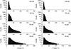 |
Fig. A.1. Deposited charge histogram of the A (on the left-hand section) and C (on the right-hand section) SiC-based diodes for power ranging from 20 to 250 kW and neutron fluences from around 3.2 × 10¹⁵ to 6.6–7.6 × 1016 cm−2 with 100k pulses recorded, and for a bias voltage of −400 V. |
Cite this article as: Valentin Valero, Laurent Ottaviani, Abdallah Lyoussi, Christophe Destouches, Vladimir Radulović, Luka Snoj, Adrien Volte, Michel Carette, Christelle Reynard-Carette. In-core thermal and fast neutron measurements with 4H-SiC P+N junction diodes in the JSI TRIGA Mark II research reactor, EPJ Nuclear Sci. Technol. 11, 23 (2025). https://doi.org/10.1051/epjn/2025024.
All Tables
Count rates (s−1) of the A and B SiC-based diodes for five different reverse bias voltages for a reactor power of 100 W in the Triangular Irradiation Channel.
All Figures
|
Fig. 1. Schematic (cross-section on the left-hand section) and picture (top view on the right-hand section) of the two types of the studied 4H-SiC-based diodes. |
| In the text | |
|
Fig. 2. Picture of an opened housing containing one type of 4H-SiC-based diodes. |
| In the text | |
|
Fig. 3. Overall top view of the core with its different locations of the fuel elements, irradiation channels and control rods of the JSI TRIGA Mark II reactor, and with the Triangular Irradiation Channel used for the irradiation campaign (in red). |
| In the text | |
|
Fig. 4. Pictures showing the positioning of the two SiC-based detectors in the TIC thanks to the detector holders. |
| In the text | |
|
Fig. 5. Schematic of the measurement chain used in the Triangular Irradiation Channel. |
| In the text | |
|
Fig. 6. Evolution of the count rates of the A (in blue) and B (in red) SiC-based diodes versus the reverse bias voltage for a reactor power of 100 W in the Triangular Irradiation Channel and with a mean temperature of around 23.1 °C. |
| In the text | |
|
Fig. 7. Count rate of the diode A with NCL (a) and diode C without NCL (b) normalized by reactor power versus the neutron fluence for power ranging from 100 W to 250 kW in the Triangular Irradiation Channel for an applied bias voltage of −400 V, and for day 1 (in black) and day 2 (in red). |
| In the text | |
|
Fig. 8. Pulses of the diode A for reactor powers of 10 kW (a) and 250 kW (b) with neutron fluences of 1.1 × 1015 cm−2 and 6.6 × 1016 cm−2 respectively, pulses of the diode C for reactor powers of 10 kW (c) and 250 kW (d) with neutron fluences of 1.1 × 1015 cm−2 and 7.6 × 1016 cm−2 respectively (bias voltage of −400 V). |
| In the text | |
|
Fig. 9. Pulse Height Distribution of the A (on the left-hand section) and C (on the right-hand section) SiC-based diodes for power ranging from 20 to 250 kW and neutron fluences from around 3.2 × 10¹⁵ to 6.6–7.6 × 1016 cm−2 with 100 k pulses recorded, and for a bias voltage of −400 V. |
| In the text | |
|
Fig. 10. Rise and decay times at 90% mean values for the two SiC-based diodes (A and C) as function of neutron fluence for a bias voltage of −400 V. |
| In the text | |
|
Fig. A.1. Deposited charge histogram of the A (on the left-hand section) and C (on the right-hand section) SiC-based diodes for power ranging from 20 to 250 kW and neutron fluences from around 3.2 × 10¹⁵ to 6.6–7.6 × 1016 cm−2 with 100k pulses recorded, and for a bias voltage of −400 V. |
| In the text | |
Current usage metrics show cumulative count of Article Views (full-text article views including HTML views, PDF and ePub downloads, according to the available data) and Abstracts Views on Vision4Press platform.
Data correspond to usage on the plateform after 2015. The current usage metrics is available 48-96 hours after online publication and is updated daily on week days.
Initial download of the metrics may take a while.